| CS-534: Packet Switch Architecture
Fall 2001 |
Department of Computer Science
© copyright: University of Crete, Greece |
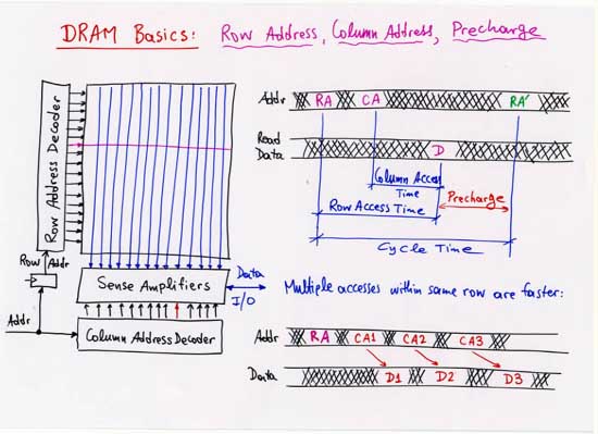
(a) Detailed Examples in an Older Technology:
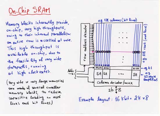
The plots, below, show examples of
cost (area, power) and performance (cycle time)
for on-chip static RAM blocks,
as functions of capacity, number of ports, and port width.
These examples are inspired by and representative of
various 0.35-micron CMOS technologies of about 1996 to 1998.
Today (2001), they are outdated,
but the detailed figures in these plots
are useful in studying how memory size and width
affect the cost and performance.
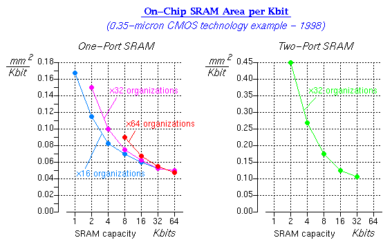
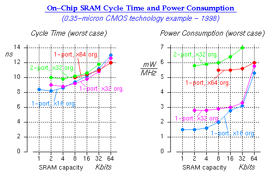
Notice that the cycle time and power figures given are for the worst case; power consumption for 2-port memories is for both ports.
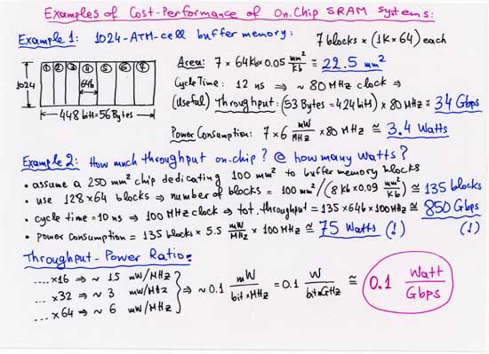
(b) Some Examples in two Current Technologies:
The cost and performance figures below
are for a couple of SRAM configuration examples
in two modern (2001) technologies
-- 0.18-micron CMOS (usual modern technology)
and 0.13-micron CMOS (aggressive and expensive modern technology).
Fabrication is by
Virtual Silicon Technology, Inc.
and can be provided to the Univ. of Crete by the
Europractice
IC Service (members of the Univ. of Crete,
please do not contact either of the above directly,
but instead go through the local Europractice representatives
by sending e-mail to
europractice@csd.uoc.gr).
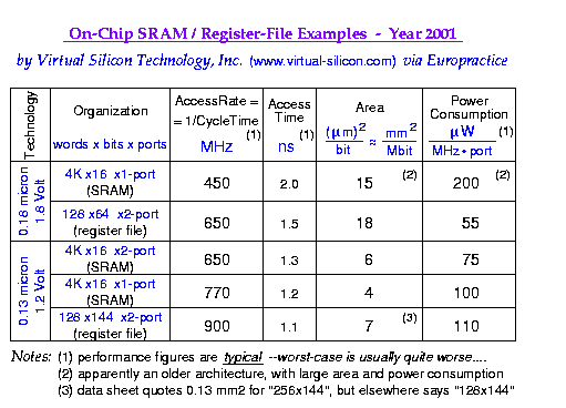
Notice that the cycle time and power figures given are for the typical case --the worst-case numbers are usually quite worse, may be as much as by a factor of two.... Also, power consumption for 2-port memories is per-port.
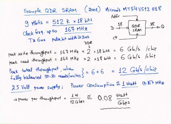
Reference: the "QDR Partnership" Web Site: http://www.qdrsram.com/.
![]()
Reference 1: Micron "MT54V 512H 18" 512 K x 18 bit (9 Mbit) QDR SRAM: PDF data sheet available on-line. For product availability information see the Component Selector Guide.
Reference 2 (Jan. 2002): Alpine Microsystems plans to introduce (Q1-Q2 of 2002) the "PacketRAM Family" of pipelined QDR SRAMS, offering 96 Gbps at 333 MHz, and higher speeds later on.
![]()
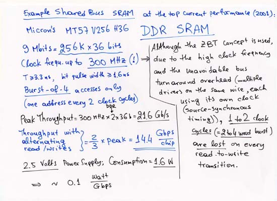
Reference: Micron "MT57V 256H 36" 256 K x 36 bit (9 Mbit) DDR SRAM: PDF data sheet available on-line. For product availability information see the Component Selector Guide.
![]()
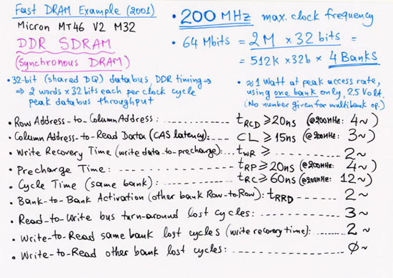
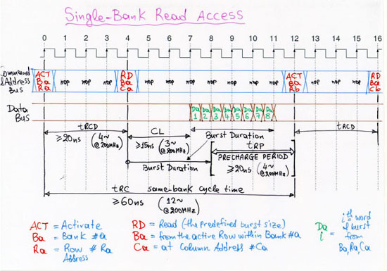
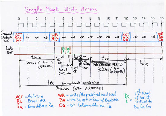
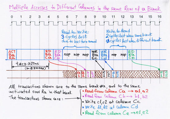
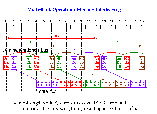
Reference: Micron "MT46V 2M 32" 2 M x 32 bit (64 Mbit) DDR SDRAM: PDF data sheet available on-line. For product availability information see the Component Selector Guide.
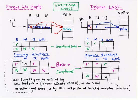
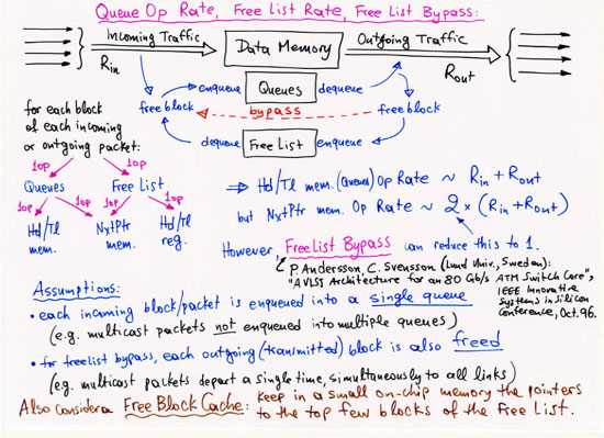
See Exercises 4 and Exercises 5 for a discussion of how large the segment (block) size should be.
Reference: A. Nikologiannis, M. Katevenis: "Efficient Per-Flow Queueing in DRAM at OC-192 Line Rate using Out-of-Order Execution Techniques", Proc. IEEE Int. Conf. on Communications (ICC'2001), Helsinki, Finland, June 2001, pp. 2048-2052; http://archvlsi.ics.forth.gr/muqpro/queueMgt.html
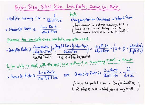
See also Exercises 4 and Exercises 5 for discussions on segment (block) size and access rate.
| Up to the Home Page of CS-534 |
© 2001 copyright: University of Crete, Greece.
Last updated: 30 Jan. 2002, by M. Katevenis. |