| CS-534: Packet Switch Architecture
Spring 2004 |
Department of Computer Science
© copyright: University of Crete, Greece |
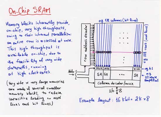
2.2 On-Chip SRAM and Power Consumption
|
[Up - Table of Contents] [Prev - 2.1 Time Switching] |
[2.3 Off-Chip Memory - Next] |
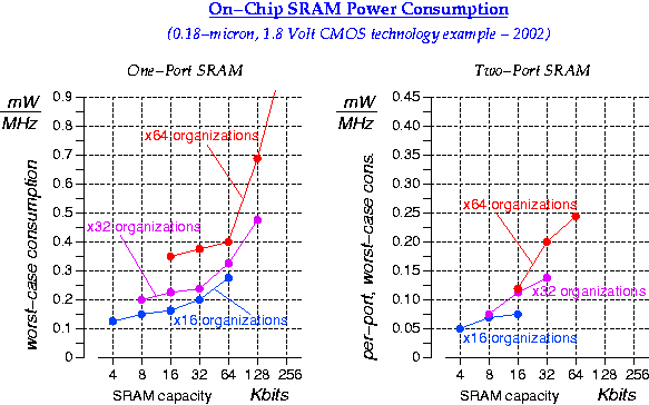
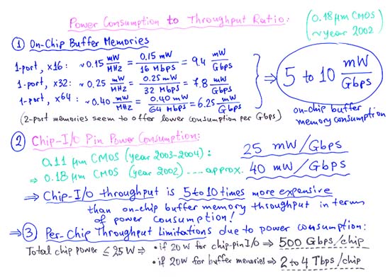
Note: power consumption of two-port memories appears to be quite lower than their corresponding one-port SRAM. Normally, one would expect the per-port consumption to be similar in 1-port or 2-port memories of the same capacity and port-width. One difference between the ports in each configuration is that the single port in 1-port memories is bidirectional, while each port in these 2-port memories is unidirectional (one port is dedicated write-port, the other is dedicated read-port); it is hard for this difference by itself, though, to account for just a large discrepancy in power consumption. The reasons for this large difference are still under investigation.
Another data point says that a typical transceiver for the two differential pairs comprising a bidirectional 3.125 GBaud (2.5 Gbit/s) link consumes approx. 300 mW when the signals are intended to cross about a meter of distance or so (over copper); attenuation and signal pre-emphasis depend on the distance that you want the signals shipped at, hence so does transceiver power consumption.
|
[Up - Table of Contents] [Prev - 2.1 Time Switching] |
[2.3 Off-Chip Memory - Next] |
| Up to the Home Page of CS-534
|
© copyright
University of Crete, Greece.
Last major update: March 2003 (minor: 18/3/04), by M. Katevenis. |