| CS-534: Packet Switch Architecture
Spring 2005 |
Department of Computer Science
© copyright: University of Crete, Greece |
2.2 Off-Chip Memory Technologies
|
[Up - Table of Contents] [Prev - 2.1 On-Chip SRAM, Power] |
[2.3 Time Switching - Next] |
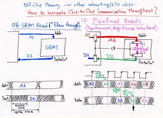
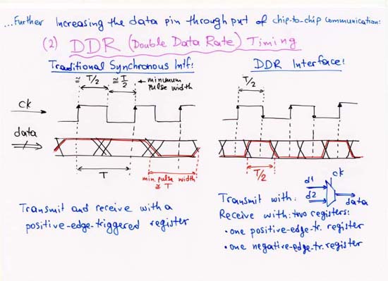
2.2.1 Synchronous RAM Chip Interfaces, DDR Timing
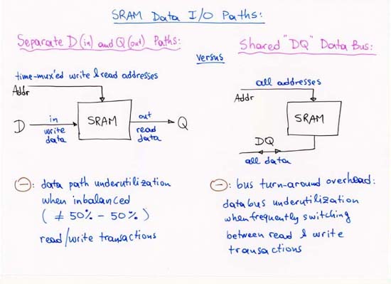
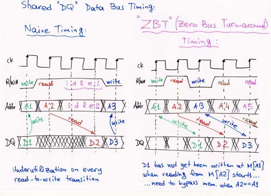
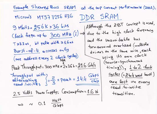
2.2.2 Bus Turn-Around Overhead Minimization
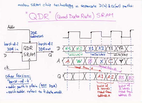
Reference: the "QDR Partnership" Web Site: http://www.qdrsram.com/.
![]()
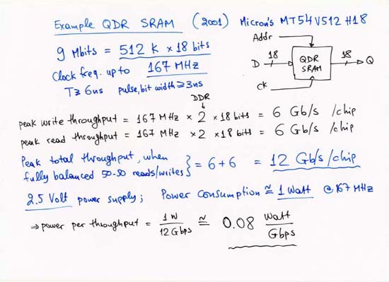
Reference 1: Micron "MT54V 512H 18" 512 K x 18 bit (9 Mbit) QDR SRAM: PDF data sheet available on-line. For product availability information see the Component Selector Guide.
Reference 2 (Jan. 2002): Alpine Microsystems plans to introduce (Q1-Q2 of 2002) the "PacketRAM Family" of pipelined QDR SRAMS, offering 96 Gbps at 333 MHz, and higher speeds later on.
![]()
Reference: Micron "MT57V 256H 36" 256 K x 36 bit (9 Mbit) DDR SRAM: PDF data sheet available on-line. For product availability information see the Component Selector Guide.
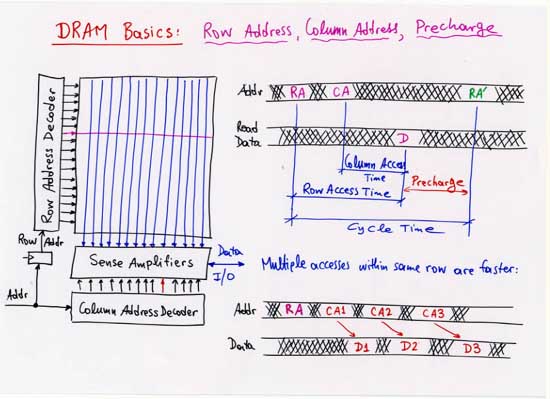
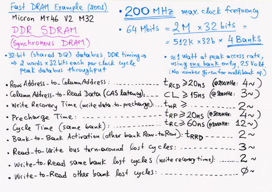
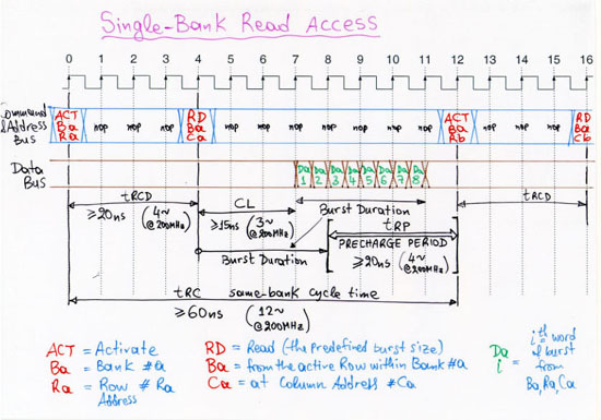
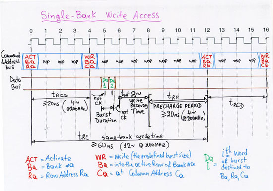
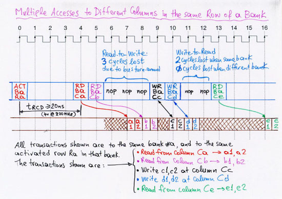
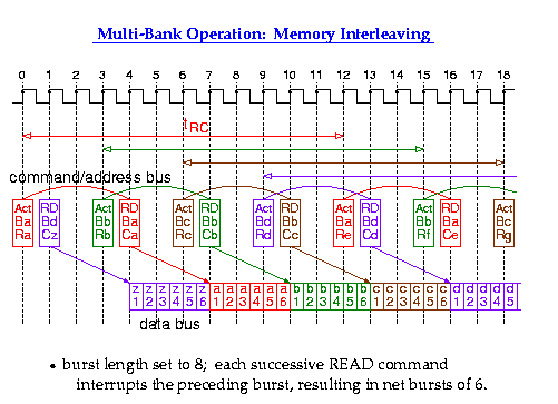
2.2.3 Dynamic RAM, Internal Bank Interleaving
![]()
Reference: Micron "MT46V 2M 32" 2 M x 32 bit (64 Mbit) DDR SDRAM: PDF data sheet available on-line. For product availability information see the Component Selector Guide.
|
[Up - Table of Contents] [Prev - 2.1 On-Chip SRAM, Power] |
[2.3 Time Switching - Next] |
| Up to the Home Page of CS-534
|
© copyright
University of Crete, Greece.
Last updated: 17 Apr. 2005, by M. Katevenis. |